Application
EBR (Edge Bead Removal Inspection)
EBR Inspection
- Fast defect detection
- Black and white photos: 300 Photos/Sec
- Color photos: 3~5 Photos/Sec. (Depends on distance)
- Shot: 360˚clear defect images are provided
Wafer Edge Inspection
EBR Inspection of Wafers
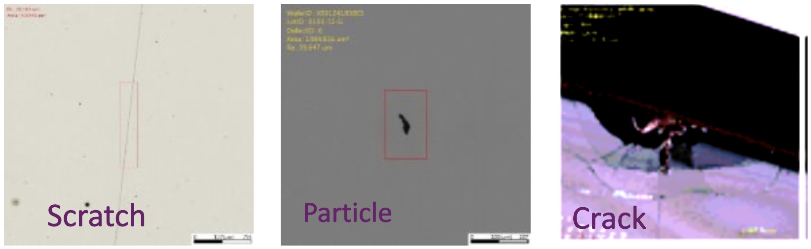
- EBR defects
- Shot Map
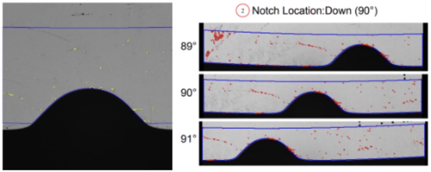
- Notch area algorithm
EBR Inspection
Inspection (Notch Area)
- The software algorithm has a built-in function to automatically determine the notch position, which only captures defects outside the notch for defect data output and judgment.
Inspection (Notch Area)
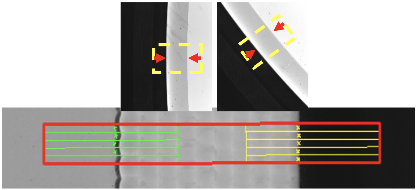
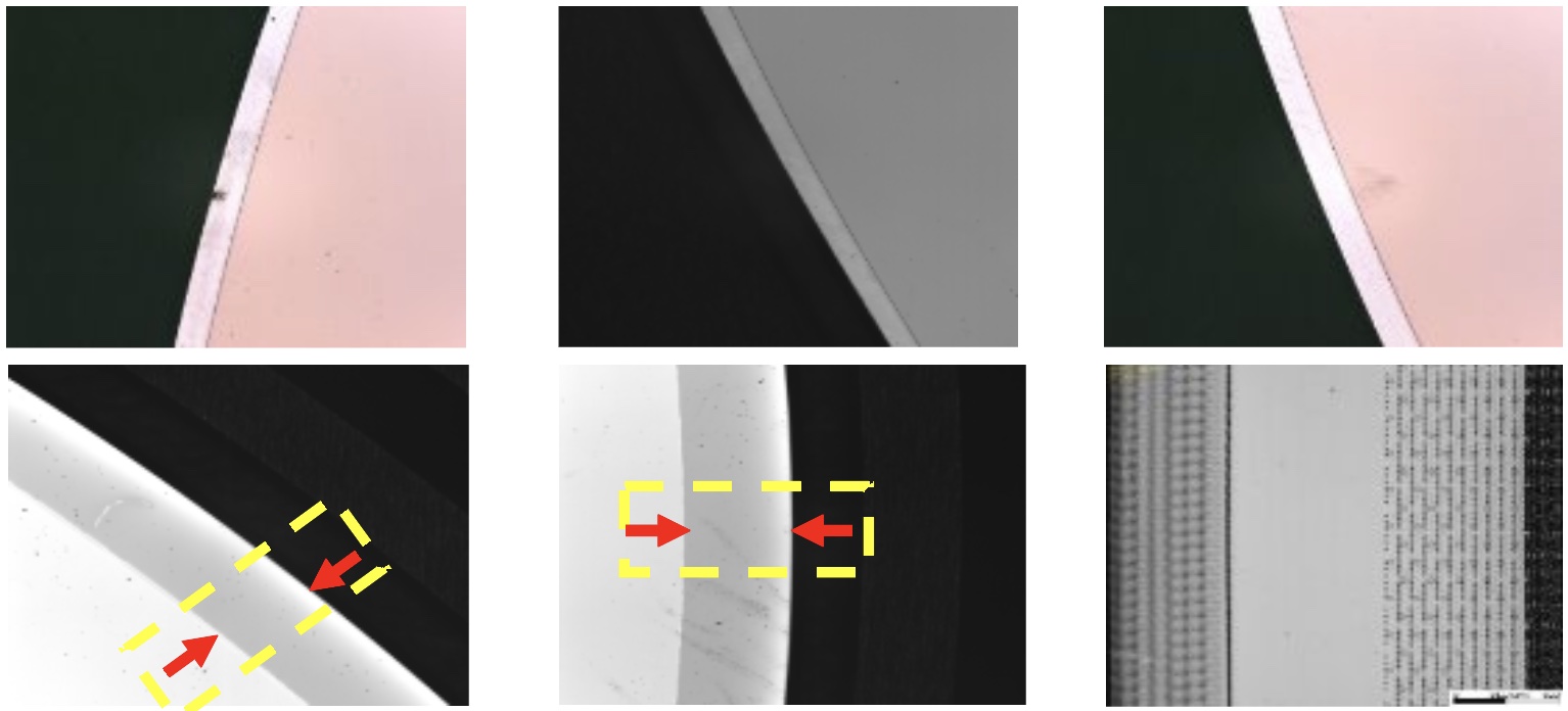
Metrology
- Precise edge computing capability
- Removed Photoresist Width Measurement
- Different angle lenses can be switched
Precise Edge Detection and Calculation