SEMI
CPO (Co-Packaged Optics)
Co-Packaged Optics (CPO) is a next-generation advanced semiconductor packaging technology that enables high-level integration of electronic components—such as switching ASICs and other high-bandwidth network processors—with optical components, including optical transceivers and laser sources, at the package level.
Through this close integration, CPO significantly shortens interconnect distances, increases system integration density, and delivers substantial improvements in data transmission bandwidth while reducing power consumption and latency. By overcoming the performance limitations of traditional electrical interconnects in high-speed data transmission, CPO has emerged as a key development focus across both the semiconductor and optical communications industries, driven by the continued growth of data centers, cloud computing, and high-speed networking.
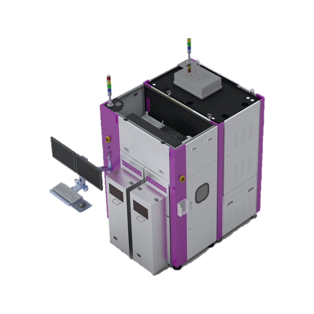
Under extremely tight spacing and stringent process conditions, alignment errors, non-uniform thickness of III–V compound semiconductor films, as well as surface or structural defects, can directly impact optical coupling efficiency and process stability, thereby increasing the risks associated with high-volume manufacturing. As a result, effective inspection and metrology of critical optical dimensions (Optical CD), III–V thin-film thickness, and optical structural defects have become indispensable elements in CPO process development and production ramp-up.
By deploying high-precision inspection and metrology solutions, manufacturers can effectively mitigate CPO process risks, establish robust and data-driven process control frameworks, and ultimately achieve reliable, high-throughput heterogeneous integration manufacturing.