SEMI
Bumping
As advanced packaging technologies continue to evolve, bump dimensions have scaled down to the μbump level, accompanied by continued pitch reduction, significantly increasing the challenges of process control and quality management. μbumps are critical structures in high-density stacking architectures such as 2.5D / 3D IC and HBM, and their quality and reliability directly impact bonding integrity and overall yield performance.
In μbump processes, bump diameter (Bump CD), bump height, and coplanarity are among the most critical metrology parameters. In parallel,defect inspection for missing bumps, shape anomalies, residues, and particle contamination is essential to ensure reliable bonding. As feature sizes continue to shrink and interconnect density increases, the demands on inspection resolution, metrology accuracy, repeatability, and high-volume manufacturing stability continue to rise.
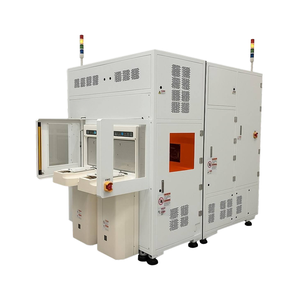
CMIt provides integrated μbump inspection and metrology solutions, enabling precise defect inspection as well as accurate measurement across full-wafer and full-panel. By helping clients monitor process variations and strengthen process control, CMIt supports stable ramp-up and high-yield manufacturing in advanced packaging applications.