μ LED
µLED
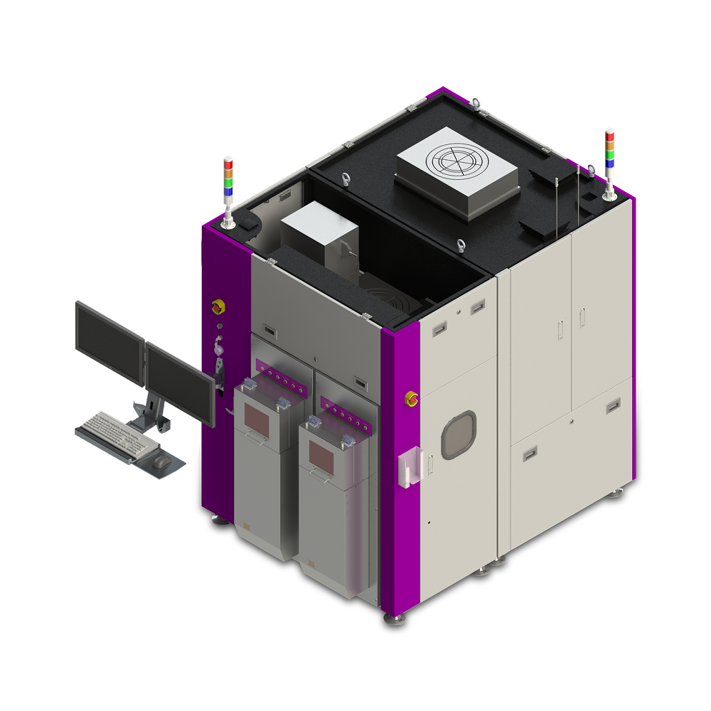
As Micro LED enters the commercial mass production stage, ensuring "zero defects" in millions of micrometer-sized wafers and achieving ultimate light quality control has become an unavoidable challenge in the manufacturing process.
This system is specifically tailored for the Micro LED industry, employing a submicron-level high-resolution optical architecture to provide a comprehensive inspection solution from epitaxial wafers and mass transfer to panel repair. To meet the stringent requirements of the COC (Chip-on-Chip) process, we innovatively integrate high-resolution AOI and advanced PL (photoluminescence) modules onto a single platform. Furthermore, we offer a precision substrate topology metrology solution that accurately captures key physical parameters including BOW, WARP, and TTV. (GSS)